September 15, 2021
Elephantech Inc.
Elephantech now Accepting Orders for our Thick Copper Trace
P-Flex® PI Utilizing High-speed Electroless Plating
Elephantech Inc. (headquarters: Chuo-ku, Tokyo, CEO: Shinya Shimizu, hereinafter “Elephantech”) is pleased to announce that, as of September 15, the company has started accepting orders for its Thick Copper Trace P-Flex® PI utilizing high-speed electroless plating.
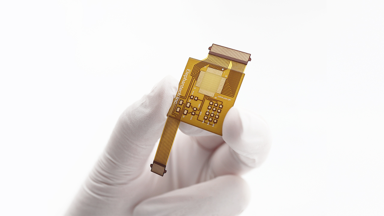
The latest addition to Elephantech's product lineup, the Thick Copper Trace P-Flex® PI
Background of this product release
Over the years, we have received much feedback from our many P-Flex® customers on how a thicker copper trace would expand the scope of applications for P-Flex® by making it capable of handling higher current values and suppress voltage drops. Generally speaking, there has been a trend for thinner copper traces in Flex PCBs. However, depending on the usage environment, there are situations in which the use of conventional P-Flex® is limited by the thinness of its trace. As a solution to these issues, we have decided to add this Thick Copper Trace P-Flex® PI to our product lineup.
Technically, as with the existing P-Flex®, silver is inkjet printed onto the substrate and electroless copper plating is applied on top. This electroless copper plating is a mechanism in which the inkjet-printed silver acts as a catalyst for the electroless copper plating with the copper growing only where silver has been printed. This requires the following three elements: "Uniformity", or uniform growth in areas where silver has been printed, "Selectivity", to have no growth where silver hasn't been printed, and "High-speed" for rapid growth. Although growing a thick copper trace had already been possible at an R&D level, we had yet to bring it to market as we were unable to successfully balance these three elements at mass production level. As such, 3µm had been the limit in terms of copper trace thickness we could supply at mass production level.
To overcome these challenges and leading into today's release, we optimized both our printing and plating processes to simultaneously achieve all three of the above elements at mass production level even for copper traces with a thickness of 12µm.
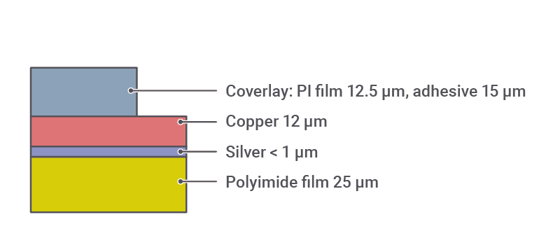
Figure The layer structure of the Thick Copper Trace P-Flex® PI newly added to the lineup
Thick Copper Trace P-Flex® PI
Existing product
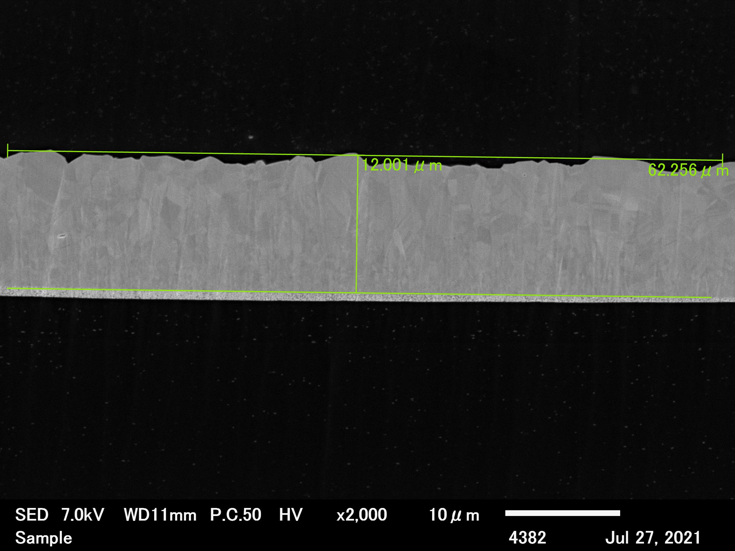
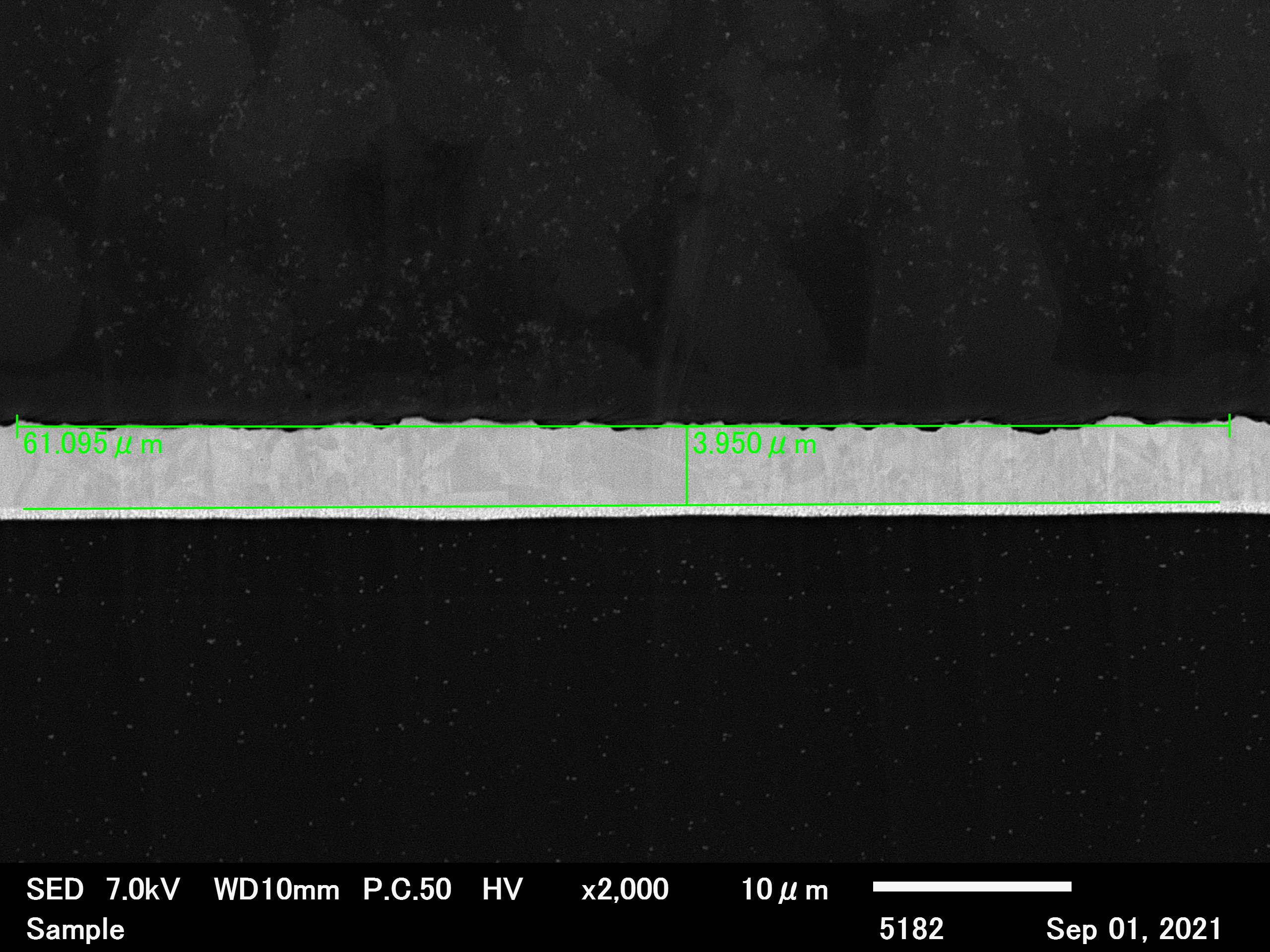
Figure Cross-sectional scanning electron microscopy of the Thick Copper Trace P-Flex® PI and the existing product
We are constantly working on increasing our product lineup so that P-Flex® PI can be used by an ever increasing number of customers, so please feel free to contact our P-Flex Sales Department or our distributors for more information or clarification on upcoming products.
With a mission to "Making the world sustainable with new manufacturing technologies", we spare no effort in our attempts to make any little contribution to the development of the electronics industry, and we are truly grateful for the continued support and interest we receive as none of this would be possible without it.
The results of this research were obtained in part from a project subsidized by the New Energy and Industrial Technology Development Organization (NEDO).
(This document was edited at 17:00 JST on September 15, 2021 for inaccuracies.)
Company Overview
| Name | Elephantech Inc. |
| Establishment | January 2014 |
| Headquarters | 4-3-8 Hatchobori, Chuo-ku, Tokyo 104-0032, Japan |
| Representative | Shinya Shimizu, CEO |
| Capital | JPY 100 million |
| Number of employees | 59 |
| Business Description | Development of printed electronics manufacturing technology and provision of related services |
| URL | https://www.elephantech.co.jp/en/ |
As of September 1, 2021
Contact for inquiries regarding this matter
Elephantech Inc. Public Relations